(China (Mainland))

Product Summary
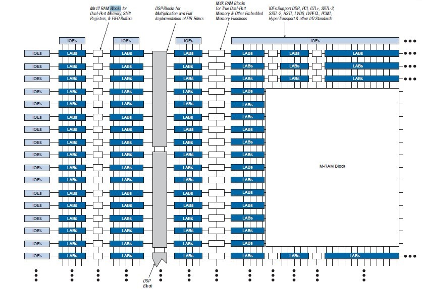
The EP1SGX25FF1020C5 contains a two-dimensional row- and column-based architecture to implement custom logic. A series of column and row interconnects of varying length and speed provide signal interconnects between logic array blocks (LABs), memory block structures, and DSP blocks. The logic array consists of LABs, with 10 logic elements (LEs) in each LAB. An LE is a small unit of logic providing efficient implementation of user logic functions. LABs are grouped into rows and columns across the device. M512 RAM blocks are simple dual-port memory blocks with 512 bits plus parity (576 bits). The EP1SGX25FF1020C5 provides dedicated simple dual-port or single-port memory up to 18-bits wide at up to 318 MHz. M512 blocks are grouped into columns across the device in between certain LABs.
Parametrics
EP1SGX25FF1020C5 absolute maximum ratings: (1)VCCINT Supply voltage: -0.5 to 2.4 V; (2)VCCIO: -0.5 to 4.6 V; (3)VI DC input voltage (3): -0.5 to 4.6 V; (4)IOUT DC output current, per pin: -25 to 25 mA; (5)TSTG Storage temperature No bias: -65 to 150 ℃; (6)TJ Junction temperature BGA packages under bias: 135 ℃.
Features
EP1SGX25FF1020C5 features: (1)High-speed serial transceiver channels with CDR provides; (2)500-megabits per second (Mbps) to 3.1875-Gbps full-duplex; (3)operation; (4)Devices are available with 4, 8, 16, or 20 high-speed serial; (5)transceiver channels providing up to 127.5 Gbps of full-duplex; (6)serial bandwidth; (7)Support for transceiver-based protocols, including 10 Gigabit Ethernet attachment unit interface (XAUI), Gigabit Ethernet(GigE), and SONET/SDH; (8)Compatible with PCI Express, SMPTE 292M, Fibre Channel, and Serial RapidIO I/O standards; (9)Programmable differential output voltage (VOD), pre-emphasis, and equalization settings for improved signal integrity; (10)Individual transmitter and receiver channel power-down capability implemented automatically by the QuartusR II software for reduced power consumption during non-operation; (11)Programmable transceiver-to-FPGA interface with support for 8-, 10-, 16-, and 20-bit wide data paths; (12)1.5-V pseudo current mode logic (PCML) for 500 Mbps to; (13)3.1875 Gbps; (14)Support for LVDS, LVPECL, and 3.3-V PCML on reference; (15)clocks and receiver input pins (AC-coupled); (16)Built-in self test (BIST); (17)Hot insertion/removal protection circuitry; (18)Pattern detector and word aligner supports programmable; (19)patterns; (20)8B/10B encoder/decoder performs 8- to 10-bit encoding and 10-to 8-bit decoding; (21)Rate matcher compliant with IEEE 802.3-2002 for GigE mode and with IEEE 802-3ae for XAUI mode; (22)Channel bonding compliant with IEEE 802.3ae (for XAUI mode only); (23)Device can bypass some transceiver block features if necessary.
Diagrams
| Image | Part No | Mfg | Description |  |
Pricing (USD) |
Quantity | ||||||
|---|---|---|---|---|---|---|---|---|---|---|---|---|
 |
 EP1SGX25FF1020C5 |
|
IC STRATIX GX FPGA 25K 1020-FBGA |
Data Sheet |
|
|
||||||
|
EP1SGX25FF1020C5N |
|
IC STRATIX GX FPGA 25K 1020-FBGA |
Data Sheet |
|
|
||||||